

Explaining the Oxygen Challenge for High Resistivity P-type Silicon Wafers
The main challenge for higher resistivity silicon material is to control the behavior of interstitial oxygen involved during the growth of Si crystals. The concentration of interstitial oxygen is generally higher than 5E17at/cc and it can be converted beneficially into oxygen precipitates below the area to eliminate metallic contaminants away from active devices.
In P-type silicon wafers, thermal donors used to increase the resistivity of the Si wafer until the concentration of the thermal donor exceeds the P-type carrier concentration. At this point, the wafer will appear to be n-type. Calculations here are generally based on experimental data illustrating the influence of thermal donors. It is shown on a 50 ohm-cm P-type wafer resistivity for different interstitial oxygen levels.
Chemical and crystallographic defects are a reality of solar-grade silicon wafers and industrial production processes. As we all know Silicon is a commonly used semiconductor, which means that it has a high resistance to the electricity. However, the resistance is not as high as an insulator such as rubber. Pure silicon used to have electrical properties, which are manipulated by other elements and called “dopants”. These dopants determine the type of silicon, positive or negative, and also change the resistivity of the silicon.
Dopants basically decide whether the final Si wafer will be a P-type wafer or an N-type wafer. Furthermore, the amount of dopant determines the final resistivity of the wafer. P-type silicon wafer are manufactured by using only one type of dopant, called as Boron, which you can also see in the periodic table as B. The volume of Boron present in the silicon wafer determines the resistivity. It is believed that the less Boron present in Si wafer means higher the resistivity. The relative abundance of P-type silicon wafers tends to keep the cost less than N-type wafers.
How to consider the cost of Si Wafers?
Each Si wafer must be particle-free. If there is a single particle on a polished wafer, it will adversely affect the functionality of the wafer. Due to this, calibration usually involves a traceable particles standard in order to determine the quality and cost of the fabric. There are different grades used to classify wafers. If wafers are larger than one hundred and fifty millimeters, then it usually is divided into test and mechanical test varieties.
However, Mechanical test varieties are used predominantly for equipment designed for testing and have an influence on structural and dimensional characteristics. A monitor wafer, also known as process test wafers is used in semiconductor fabrication and process monitoring. Particle silicon wafers are mainly designed to be used for measuring the actual particles. You must understand the difference between n and p-type silicon wafers to navigate the market and make price comparisons easier.
The Si wafer manufacturing process is highly complicated and tedious. It includes a number of sequential processes that are required to create an electronic circuit. As the demand for semiconductors will increase continuously in the future, manufacturing companies to speed up the manufacturing process to handle the demand.
If you are involved in the Si wafer manufacturing industry, then it is important for you to understand the complete manufacturing process. Just like with any products, quality and price vary, and the same applies on silicon wafers. It is highly advisable to learn about p-type silicon wafers in order to determine its resistivity and right usage. You can begin your research online, and find out numerous silicon wafer manufacturers in your area. Contact multiple manufacturers to get the best quote available for your work and take decision accordingly.
Similar Articles
Choosing metal testing equipment? Learn which properties, test locations, sample prep and total costs to weigh before you buy. Read our guide first.
Discover why sanitary fabrication matters in food processing facility upgrades, improving hygiene, food safety, equipment durability, and regulatory compliance.
An efficiently operating manufacturing business involves more than making good products. Good organization is key to keeping costs under control, meeting deadlines, ensuring quality, and reacting promptly to changes.
Learn how to design closed die forging with the right parting lines, draft angles, and critical details to improve manufacturability, quality, and efficiency.
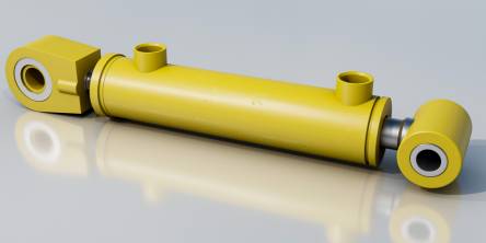
Spot the top 7 warning signs your heavy equipment needs hydraulic cylinder repair, from oil leaks to drift, and learn when to book an inspection.
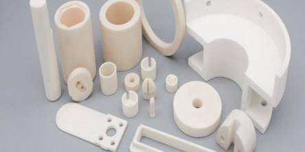
A worn guide, an overheated insulator, or a component that reacts with a cleaning solution can disrupt an otherwise reliable machine. These problems often begin with a material choice that was reasonable during development but becomes unsuitable under actual operating conditions.
Learn about HVAC sheet metal fabrication, including its key processes, materials, applications, and benefits for efficient heating and cooling systems.
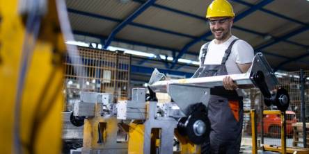
Walk through almost any manufacturing plant and you'll hear the motors before you notice the gearboxes bolted next to them. That's kind of the point
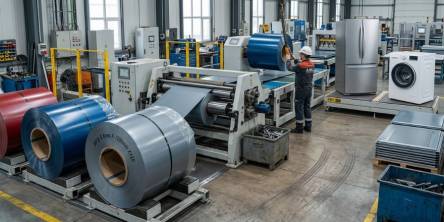
Learn how prepainted steel panels resist corrosion, scratches, UV exposure, forming stress, and finish inconsistency in home appliance manufacturing.